Aided by appropriate semiconductor diodes and transistors, solar panels are leading the way among renewable energy sources.
Over the past twenty years, sustainable energy has evolved significantly. Improvements in renewable energy technology have led to higher power conversion efficiency, with high projected growth rates over the next ten years in the automobile and commercial power markets. Leading the way among the various renewable energy sources are solar panels, which are popular due to their ease of accessibility.
Along with accessibility, solar panel power conversion efficiency (PCE) has greatly improved since its inception, with modern consumer panels capable of outputting a 22% figure. In order to achieve a high PCE, solar panel networks feature bypass diodes. These diodes are used to prevent unwanted power consumption and hotspotting when cell shading occurs, thereby allowing the panels to efficiently generate current. The generated current is direct current (DC), which is then converted to alternating current (AC) by an inverter, and ultimately transferred to a power grid. From this point on, appliances and tools draw this AC signal from the power grid. Depending on the powered device, the AC signal may be converted to DC, which is often further modified by means of a DC-DC converter.
Bypass diode implementation
In a normal operating state, solar cells convert incident solar radiation into electric current, essentially acting as sources. If a cell in the string was to malfunction, however, the cell would instead become an electrical impedance. The most common solar cell malfunction is cell shading, which unfortunately is unavoidable; cell shading can quickly become fatal to the solar cell network. The shaded cell(s) will begin to drop voltage rather than source current. This leads to hotspotting, since the shaded cell(s) dissipate a large amount of the power generated by the working cells.
Hotspotting will likely damage or destroy the shaded cell(s) and could potentially cause an environmental hazard. Even if there is no damage to the system, there is still a significant power loss, which causes the overall PCE to decrease. In order to avoid this scenario, bypass diodes are placed in parallel with solar panel cells. Under normal operation, these bypass diodes are reverse biased and will not interfere with circuit operation. In the case of cell shading, the bypass diodes provide an alternate, low-resistance path for current. While the overall power generated by the system will still be lower, there is no damage to the working or shaded cell(s). In an ideal design, each cell would have its own bypass diode. However, due to cost implications, bypass diodes are typically placed in parallel with anywhere from 10 to 20 series cells.
Schottky rectifiers are the recommended technology type for bypass diodes. The fast switching properties and low forward voltage of Schottky rectifiers help solar cell networks maintain a relatively lossless performance. Central manufactures multiple Schottky rectifiers—both through-hole and surface mount packages—that meet desired bypass diode specifications. Typically, a bypass diode has a reverse breakdown rating between 60V and 100V, more than enough to block the combined cell voltages in normal operation. For forward conduction, the bypass diode must conduct the large amount of current that is generated by the active cells. This current range can vary depending on application, making Schottky diodes that can rectify 6A or higher an ideal solution.
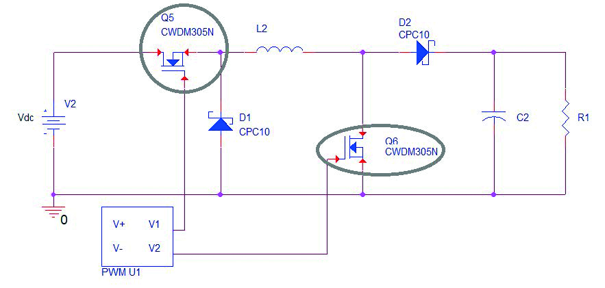
MOSFETs in inverters and DC-DC converters
The direct current generated by the solar cell network must be converted to alternating current before it can be delivered to a power grid. This is done through the use of inverters, which are switching circuits comprised of MOSFETs. Four N-Channel MOSFETs are used in the standard DC to AC inverter topology, where two parallel branches of two series MOSFETs are connected via a common load. Two of the four MOSFETs are switched on and off such that current across the load produces a natural half-square wave.
In order to produce a half-sine wave rather than a half-square wave, a pulse-width modulator (PWM) can be used to drive the MOSFET gates. PWMs are controlled drivers that have a modifiable pulse width, which is executed using comparator topology. Modifying the pulse width that drives the MOSFET gates regulates how long each MOSFET is switched on or off. The less time a MOSFET is switched on, the lower the duty cycle of the load current. By modifying the pulse width over time, the load current can be averaged as a half sine wave, with short pulses producing low amplitude portions and long pulses producing high amplitude portions.
After the formation of the half sine wave, the two MOSFETs that were open during the first half of the period are used in the same manner as the previous two. They are switched on and off so that current across the load produces a natural-half square wave, except load current direction is reversed. Combining the two generated signals creates a full sine wave that can be stepped-up or stepped-down with a transformer used for power distribution.
Appliances and electronics that use DC power must convert the AC signal from the grid back to DC. This is completed through standard AC-DC rectification using a bridge rectifier, load, and smoothing capacitor. After rectifying back to DC, there is often a DC-DC stage used to either boost or buck the DC signal. This sets the DC voltage level in order to ensure its compatibility with the power requirements of the given device. Both boost and buck DC-DC converters make use of switches, often MOSFETs, to alter the path of current flow. By changing the available path to the current within the circuit, the inductive element of the converter will reverse polarity and in-turn alter the output signal.
Implementing SiC Schottkys in DC-DC converters
Aside from the MOSFETs and passive components necessary to design a DC-DC converter, Schottky diodes are required to regulate current flow. Schottkys are often selected for this type of asynchronous design because they can turn on and off very quickly, leading to higher levels of efficiency due to low energy loss. In boost mode, only one Schottky diode is required. When the MOSFET is switched off and the inductor flips polarity, the Schottky diode turns on and allows forward conduction to the load. In buck mode, two Schottky diodes are required. When the MOSFET is switched off and the inductor flips polarity, one Schottky diode conducts to the load—just as with the boost converter—and the other Schottky diode provides a path from ground to the inductor, acting as a battery in the circuit.
Rather than use standard Schottky diodes, silicon carbide (SiC) Schottky diodes can be used in DC-DC converters to ensure a more efficient design. This is due to the innate material composition of silicon carbide as well as its wide bandgap potential of 3.26eV. Since the bandgap shrinks with temperature increase, the wide starting bandgap allows SiC to remain functional in much higher temperature ranges. SiC, in turn, has an enhanced thermal conductivity of 490 W/(m*K) (6H form), which is much larger than that of silicon at 149 W/(m*K). This greatly helps to avoid increases in leakage current at higher operating temperatures.
The wide bandgap of SiC also directly contributes to another important property: high breakdown voltage potential. The critical electrical field (the required potential per meter for electrical breakdown) increases with increased bandgap potential. For this reason, the breakdown voltages of SiC Schottkys can be designed to occur in the range of 600V to 1200V, which is much higher than the 200V breakdown maximum seen in silicon Schottky processes. This makes SiC a more effective voltage blocker and less prone to high leakage currents at lower voltages.
The most enticing property of SiC however, is its lossless switching characteristics. Every silicon diode, whether standard or Schottky, takes a set amount of time to turn on and off. At high frequencies this is detrimental to operation because cumulative charge loss over multiple periods can be extremely high. SiC displays superior electron drift velocity, which is defined as electron mobility given a specific electric field potential. While intrinsic carrier mobility figures for silicon and SiC are quite similar, electron drift velocity is considered to be the key parameter due to its non-proportional change at high electric field values. The value of electron drift velocity at high electric fields of SiC can reach double that of silicon, with a top value of 2E7 centimeters per second.
Conclusion
As noted earlier, renewable energy continues to grow in popularity with strong continued growth projected throughout the next decade. Central Semiconductor is keenly aware of the importance of this growing technology and has responded by placing a large emphasis on designing devices that are both parametrically advanced and highly efficient. With the key factor being energy sustainability, an important focus of Central’s product development efforts for these applications is to design devices that are as lossless as possible. It is Central’s goal to continue supporting these applications, in addition to many others, by designing and manufacturing the most efficient and innovative discrete semiconductors in the industry.