It is no longer sufficient to simulate analog and digital blocks separately in a “divide and conquer” approach.
We are at a time when the computing performance benefits of Moore’s law are coming more slowly and at a higher cost, even as artificial intelligence (AI) applications are driving demand for extreme compute performance. According to the non-profit research firm OpenAI, the amount of compute performance used to power the largest AI training runs has increased exponentially since 2012—doubling every 3.5 months.
Data processing and computing power are moving into the cloud, which offers significant flexibility and scalability achieved by the deployment and use of massive infrastructure based on uniform computing platforms working in parallel. This infrastructure is comprised of powerful servers running the fastest processors. However, as the demands on cloud application processors continue to increase, so does the complexity of the underlying System-on-Chip (SoC) devices. New heterogeneous compute architectures are designed to bring together the CPU, GPU, and accelerators into one SoC, often in multicore configurations to accelerate specific applications and algorithms. The complexity of heterogeneous architectures is resulting in a need for more focus on how we verify and validate the functionality of these SoCs.
As design complexity has spiked, so too has the complexity of verifying these increasingly sophisticated devices. SoC verification has become an exercise of applying many unique methodologies for each of the different classes of sub-design within a design. The advent of new technologies such as constrained-random data generation, assertion-based verification, coverage-driven verification, formal model checking, and intelligent testbench automation (to name just a few), has changed the way we see functional verification productivity. However, most of these new technologies have not been extended to verify mixed-signal design challenges.
So, why do we need to worry about mixed-signal verification for these SoCs? One major reason is the fact that data centers have adopted newer processing techniques by integrating accelerators—specifically, graphics processing units (GPUs)—to support emerging AI and deep learning workloads. GPUs are high-performance, high-throughput chips that require I/O bandwidth on the order of Gbps and high-bandwidth memory interfaces. Though these GPUs can provide much-needed compute acceleration, one GPU is not enough, and so servers today often incorporate networks of 8 or 16 GPUs. The GPUs work in conjunction with the main CPU and memory, and communication between these compute processors and memory takes place over a physical interconnect.
Design and verification teams working in this space realize that the performance of the design is key, and that verifying this performance is no longer simply a digital verification exercise. The performance of these communication networks will determine the overall throughput of the system, and this can become a potential bottleneck resulting in slower response times from cloud servers. These I/O interconnects are implemented by high-speed PHYs comprised of complex mixed-signal circuitry with a significant amount of digital data interlaced with analog data. The high bandwidth memory interfaces use DDR PHYs with DLL-based clocking circuits which are very sensitive to device noise and variations in power, voltage, and temperature (PVT).
SerDes represent the basic building blocks of PHYs, and SerDes designs are always evolving, whether it is a new adaptive equalization scheme or digitally assisted analog blocks in the architecture. One of the most critical components in the SerDes is the clock generation, which is primarily performed via a phased locked loop (PLL).
In a traditional PLL, the control data is represented as an analog voltage. As all sub-blocks are vulnerable to different sources of voltage noise, the performance can easily be degraded. This is especially a problem in advanced semiconductor process nodes where supply voltages are scaled down, decreasing the voltage headroom and signal to noise ratio. Additionally, in these types of processes, analog properties such as linearity or device matching grow increasingly inferior, as analog loop filters built from resistors and capacitors are not scaling down with the technology. All of this led to the emergence of digital PLL architectures, which tend to benefit from process scaling. Despite the benefits that digital PLLs offer, there are also new challenges that arise, such as quantization errors and non-linearities in the control loop. These can degrade the performance and complicate the analysis compared to traditional PLLs.
The level of communication between the analog and digital components in today’s SerDes interconnects is vastly more complex than it was in the past. The interplay between these realms is so integral to the functionality of the SerDes that it is no longer sufficient to simulate analog and digital blocks separately in a “divide and conquer” approach. Designers must simulate these two domains collectively, utilizing an array of advanced mixed-signal verification strategies to obtain the coverage closure required for first-pass silicon success.
Simulating the behavior of a mixed-signal design requires both digital and analog solvers to work in conjunction in a synchronized fashion. In mixed-signal simulation, analog solvers become the bottleneck in meeting the overall performance goal for verification. To achieve reasonable simulation speeds, many mixed-signal engineering teams employ analog behavioral modeling. However, models are becoming more challenging to develop, incorporate, and utilize effectively at smaller technology nodes (like 5/3nm) as design complexity, process variation, and physical effects add to the number of variables that need to be considered.
In mixed-signal design, errors most often occur at the interfaces between analog and digital blocks. Mixed-signal debug gets even more complex when the design employs advanced, low-power techniques. For example, data corruption in a digital block due to faulty power sequencing can pass to an analog block, resulting in inaccurate voltage conversion. Scenarios like this are difficult to debug by analog designers who are unaware of digital low-power techniques.
Digital verification methodologies are mature, organized, and have mastered the art of automation. Analog and mixed-signal verification, on the other hand, traditionally relied on direct verification methods. While this might have been sufficient in the past, increasing complexity and design sizes necessitate more thorough and automated verification of mixed-signal SoCs. Analog verification teams must go beyond traditional methodologies like directed tests, sweeps, corners, and Monte Carlo analysis. Teams need to embrace digital verification techniques to facilitate regression testing of mixed-signal SoCs. These techniques include automated stimulus generation, coverage, and assertion-driven verification combined with low-power verification and automated debug for improved productivity.
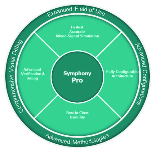
Siemens EDA offers comprehensive support for these advanced methodologies with the Symphony and Symphony Pro mixed-signal platforms. Symphony offers an average of 2 to 5X speed-up over traditional mixed-signal simulators while maintaining SPICE accuracy. It is fully configurable to work with all industry-standard digital solvers and provides robust debug capabilities within an easy-to-use environment. In addition, Symphony’s mixed-signal simulator offers a unique machine learning-based variation-aware mixed-signal solution with Solido Variation Designer.
In summary, extending the support for digital verification methodology for mixed-signal designs in modern EDA platforms is improving the coverage closure for heterogeneous SoCs, which can speed time to market.