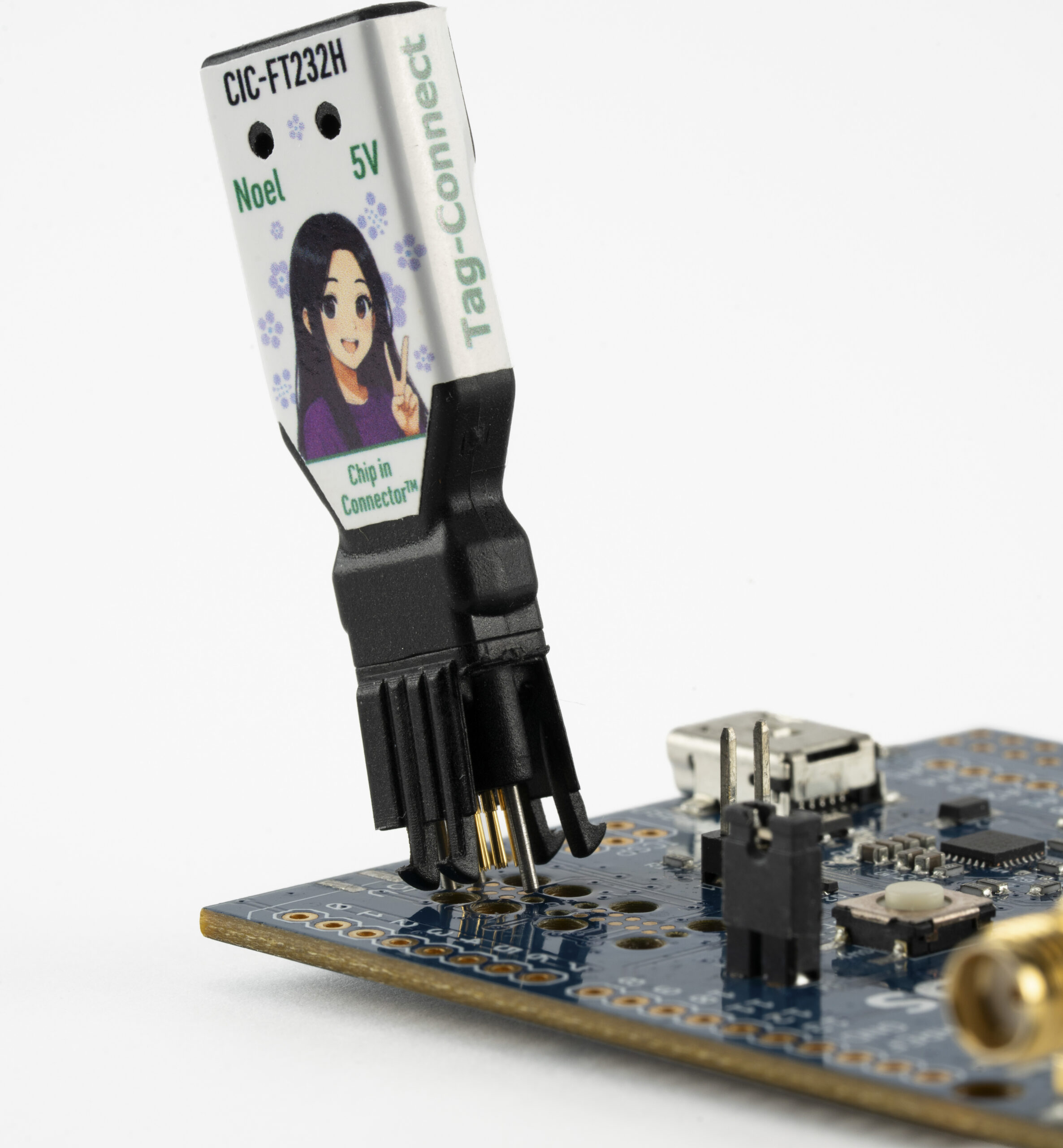
Over the last few decades, the architecture of embedded programming and debug interfaces has remained fairly consistent. A USB-connected programmer/debugger communicates with a target PCB through a ribbon or instrumentation cable connected to a programming header. Depending on the application, that connection may carry JTAG, SWD, UART, SPI or I²C signals before finally reaching the target device through PCB traces. This architecture made sense in a time when programming speeds were relatively low, PCBs were physically larger, and connectors occupied only a small proportion of the available board area.
However, embedded systems today are rather different. Programming interfaces operate at higher speeds while products themselves have become smaller, denser and increasingly constrained for both PCB space and physical height. Engineers expect the same programming interface to support development, production programming, manufacturing test, firmware updates and field diagnostics throughout a product’s life. The distance between the interface electronics and the target device has become more significant as increased speeds and growing download sizes cause a challenge to signal integrity, while routing those signals to a fixed programming header consumes valuable PCB real estate.
It seemed worth asking whether the USB should be converted into the target protocol so far from the device itself. Why not perform the conversion just a few millimetres from the target device? This approach would require integrating the USB interface electronics into the programming connector itself. Tag-Connect Plug-of-Nails™ spring-pin connectors are ideal for this task since they connect temporarily to a tiny footprint of pads and holes on the PCB, eliminating the need for the physical programming header, and allowing the programming footprint to be placed very close to the target device. Guide pins ensure accurate alignment and crown-tipped pogo-pin contacts, tested to more than 100,000 mating cycles, make secure and reliable electrical connections.
With careful electrical and mechanical design, we integrated the USB interface electronics into a compact Plug-of-Nails™ connector body, creating the Chip-in-Connector™ family of programming interfaces with integrated USB protocol conversion.
USB was specifically designed to carry high-speed data over relatively long distances using twisted pair differential signalling and overall shielding. Whereas once these signals are converted into JTAG, SWD, UART, SPI or I²C, they are typically carried over a multi-core ribbon or instrumentation cable before finally reaching the target device. While these cables perform well for many applications, the growing size of downloads and need for increased data rates make them progressively more susceptible to cable length, crosstalk, impedance discontinuities and signal degradation.
By relocating the interface electronics into the connector itself, the entire distance between the host computer and the target is carried by well-purposed USB, leaving only the final few millimetres to connect the target interface signals. The post-USB signal path is reduced substantially, improving signal integrity while reducing susceptibility to reflections, timing errors and other signal-quality issues.
The first Chip-in-Connector™ in our range utilizes FTDI’s FT232H high-speed USB to serial protocol conversion chip. While best known for USB-to-UART applications such as serial consoles and bootloaders for devices like the ESP32, the FT232H also supports JTAG, SPI and I²C. This makes it suitable for applications such as FPGA configuration, microcontroller programming and other embedded development tasks.
Typically in an FT232 interface cable, the USB to serial conversion occurs at the USB end of a less than ideal, stiff and bulky instrumentation cable. By moving the interface electronics into the connector itself, a flexible and light USB-C cable is used for the entire signal length from the host PC to the target.
The Plug-of-Nails™ technology used in this Chip-in-Connector™ allows PCB designers greater freedom during board layout and the tiny footprint remains useful throughout a product’s life cycle. During development it provides easy access for board bring-up, debugging and firmware development. For production it allows convenient programming and functional test access without the cost, space and overhead associated with a permanent connector. Later, if firmware updates or diagnostics are required, support technicians simply connect to the existing Plug-of-Nails™ footprint without needing to solder temporary wires or install a header that was intentionally omitted from production.
We encountered the practical value of this approach while working on an implantable medical device where available PCB real estate was extremely limited and a conventional programming connector was physically impossible. A roughly 0805-sized Plug-of-Nails™ footprint allowed the manufacturer to retain programming and diagnostic access throughout development, production and post-use interrogation, without increasing the product’s size. As boards continue to shrink, similar constraints are becoming increasingly common in many embedded implementations.
The broader objective of our work has not simply been to shrink the programming interface, but to revise design assumptions that no longer make sense. The challenge in developing Chip-in-Connector™ was to keep the high-speed USB connection intact while reducing the length of the lower-level target signals, balancing the trade offs between mechanical constraints, PCB layout and signal integrity. For engineers designing increasingly demanding embedded systems, moving the USB protocol conversion closer to the target device shortens the post-USB signal path, improving signal integrity while simplifying programming and test connections.