The semiconductor foundry space can be broadly classified into two dominant categories: the Digital Foundry and the Analog (or Specialty) Foundry. The Digital Foundry leverages a large capital investment into relatively standardized technology that serves a large set of customers in a uniform way and is primarily focused on scaling CMOS.
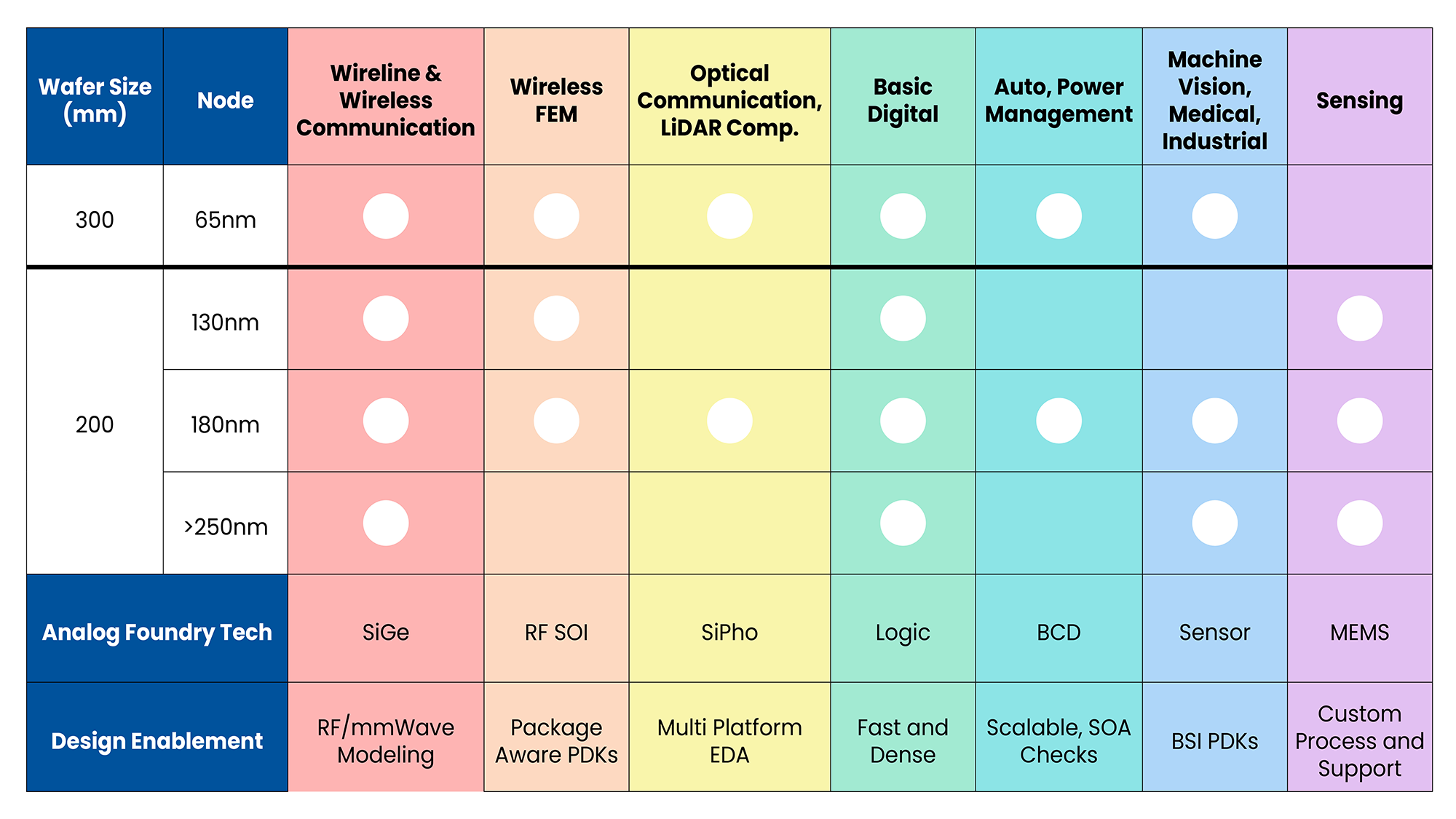
The Analog Foundry, which is the focus of this article, leverages customized technology and close design support together with a more modest capital investment to serves a rapidly growing but more custom analog markets such as those of RF, power management, silicon photonics, and sensors. Products manufactured by Analog foundries are driving features in diverse applications such as automotive, sensing, computing, and both wireless and wireline communications. In some cases, the adoption of analog foundry technologies is driven by cost, where the significantly lower NRE at mature nodes enables rapid prototyping and customization. In other cases, it is performance driven as analog components typically do not improve with scaling and therefore innovation in analog components such as SiGe bipolars, high-voltage MOSFETs, and high-performance passives have occurred in more mature lithography nodes as shown in the table below, which highlights the Analog Foundry technology offered by Tower Semiconductor.
Another trend visible from the table below, is the emergence of the 300mm wafer technologies at the 65nm node, where the features from well-established 180 and 130nm nodes are now available. These new Analog Foundry technology nodes are enabling IC design teams to package more advanced digital functionality, while taking advantage of the aggressive design rules to reduce the analog footprint when possible. An example of this in the Rds-on (the series resistance of a Power MOSFET), where the shrunk contacts and overplots can reduce the area of a driver circuit by more than 30% for similar performance. Likewise, the synthesized area of a digital MIPI block in RF SOI switch IC in a wireless FEM, can be reduced by half.
An often-overlooked capability in Analog Foundry Technology offering is related to Design Enablement. This includes silicon-verified device models and flexible design environments, allowing IC design teams to test, modify and improve the functionality and yield of new products long before the first prototype is manufactured. The role of an Analog foundry is key in enabling a design environment that is easy to install and use, while being accurate and feature-rich to enable first-time success on silicon. Some of the key features enabled by Tower Semiconductor Analog Foundry shown in the last row of the table have been developed with valuable input from fabless design customers over the last two decades. These include accurate RF models which include package aware design flows, ability to verify safe operation (SOA) of design blocks from within the design cockpit and multi-platform PDKs allowing the fabless design team to choose tools that work best for them.
In summary, the Analog Foundry is driving innovation in most areas of electronic and photonic design with cost effective solutions, leveraging well-proven mature nodes as the base.