AI introduces exciting new opportunities for productivity and collaboration in the mature discipline of PCB layout design.
Integrating artificial intelligence (AI) into various processes has become a transformative force in the rapidly evolving electronics and electrical engineering field. Within the hardware design process, PCB layout design, a pivotal facet of electronic product development, is experiencing a significant shift with the infusion of AI. Let’s dig into AI for PCB layout design to explore its profound impact on efficiency gains, its limitations, and its role as a collaborative tool.
Hardware design productivity
The digital age ushered in a wave of technological advancements, and AI’s role in hardware design is proving to be a game-changer.
Historically, PCB layout designers grappled with their craft’s repetitive activities, like component placement, trace routing, and design rule checks. These essential tasks can be both labor-intensive and mentally taxing.
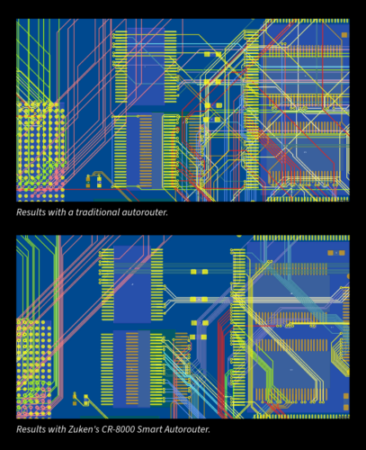
We can teach AI tools to handle these repetitive tasks. An AI tool developed specifically for PCB layout can swiftly process and analyze vast amounts of data, making optimal choices for component placement, signal routing, power distribution, and thermal management. Based on machine learning from existing successful place and route projects, the AI-generated boards will mirror past human-created PCB designs better than a traditional autorouter. While a conventional autorouter is based on algorithms, the AI-based routing engine can learn from design examples.
One of the most immediate benefits of incorporating AI into hardware design is its ability to handle complex tasks. A good example is asking an AI copilot (i.e., an AI-based utility) to optimize the BOM (bill of materials) for cost. The AI copilot can search the supply chain for equivalent and more cost-effective components. BOM optimization is a complex manual task that AI can take over and address in seconds or minutes.
The implications of this shift are profound. AI-driven automation accelerates and efficiently manages component placement, optimizing signal integrity, power distribution, and thermal management. The result? Faster time-to-market without compromising quality or functionality. In today’s fast-paced electronics industry, this acceleration is invaluable.
Training with high-quality designs
AI machine learning is essentially transferring design strategies to your next project. Companies produce various electronic products utilizing different technologies and implementation strategies. The AI engine needs to be trained on each design type and strategy. Each company or department can produce an AI tool tuned for their products and technology. Even within your company, each department can train the AI engine for their specific needs. The ability to transfer or preserve design knowledge specific to a product is a powerful concept.
Boards can contain a variety of different technologies. Consider company A, which uses DDR4 or DDR5 memory on all its boards. Company B builds communication hardware and utilizes SERDES with high pin-count FPGAs. Routing these boards requires specialized knowledge and experience. The ability to teach and create a “brain” for each technology enables the brain to identify different technologies, each with differing place and route requirements. A company can target different design types by using several trained brains (i.e., AI place and route knowledge). Training the brains with high-quality board designs will produce similar high-quality results going forward. While training with low-quality board designs will produce low-quality results. Choose your designs carefully.
Once the brain learns to place and route your board type, the process involves selecting which brain to apply and then hitting the Go button. With the AI tool as a collaborator, the place and route process is accelerated and delivers high-quality results.
Limitations of artificial intelligence
AI’s role in PCB design is not to render designers obsolete but to augment their abilities and assist with their current tasks. It acts as a powerful tool that complements human expertise. Tasks once dominated by manual labor are now executed with less human involvement, freeing designers to focus on other critical tasks.
AI does have limitations. There will be instances when the AI brain can not complete the place and route task (e.g., new technology with new routing rules). The untrained brain will struggle. The AI brain also requires computational power. A server will be necessary to analyze the board, create, and then execute a plan. For cases where the AI brain can not complete the board, human intervention will be required.
Think of AI as a copilot, ready to be part of a team to complete a specific job.
Reap the benefits
AI-based PCB layout design tools have limitations, but the benefits are clear. The often challenging and time-consuming task of placing and routing a board can be completed faster using AI to deliver human-like results. The AI tool can continually learn, making for a productive copilot. Time previously spent on place and route can be reallocated to explore new solutions and develop new skills.
Once the AI brain has been taught how to place and route a particular type of design, the brain will deliver consistent and predictable results. And it has 24/7 availability to deliver results more quickly.
The human-AI partnership
The integration of AI into PCB design marks the evolution of a collaborative partnership between human intelligence and machine learning capabilities. Think of it as having a highly skilled teammate who excels in specific tasks while complementing your unique strengths.
AI augments the creative and problem-solving abilities of PCB designers. It provides the precision and speed required for optimizing design layouts, managing complex components, and ensuring compliance with industry standards. This collaboration results in more innovative and efficient PCB designs.
Designing PCBs is both an art and a science. With its analytical prowess, AI enhances productivity by completing complex tasks with human-like results. This, in turn, allows designers to focus on creating innovative, functional, and aesthetically pleasing electronic products that get to market faster.
Embracing the future of PCB design
As we embrace the AI revolution, it’s essential to dispel the notion that AI threatens PCB industry job security. Instead, it should be viewed as a catalyst for growth and innovation in the industry. PCB designers can look forward to a future where AI enhances their roles, drives efficiency, and contributes to creating cutting-edge electronic products.
AI is not just a buzzword; it’s a valuable design ally, working hand-in-hand with PCB designers to unlock new possibilities and shape the industry’s future. By upskilling and embracing this technology, designers can confidently navigate the evolving landscape, knowing that AI is here to assist, not replace. The synergy between human ingenuity and AI capabilities is key to unlocking the full potential of PCB design.