System efficient ESD design (SEED) is a modelling methodology aiming to predict the ESD robustness of a system, evaluating transient currents and voltages during an ESD event.
According to the OPEN Alliance, Automotive Ethernet in the form of 100BASE-T1 is becoming increasingly popular and will be used by various car OEMs around the world. The OPEN Alliance is proposing a measurement called “ESD Discharge Current Measurement” which gives an estimation of the overall system-level ESD robustness of the system. This test determines the residual current into the PHY (physical layer interface), identifying the ESD robustness class according to human body model requirements.
System efficient ESD design (SEED) is a modelling methodology aiming to predict the ESD robustness of a system, evaluating transient currents and voltages during an ESD event. It is based on equivalent circuit and behavioural models. Transmission Line Pulse (TLP) and Network Analyser measurements are typically used as input for characterisation of an individual element or system part. Together with an appropriate model for the ESD generator, this methodology has been used to study ESD events on system-level elements for high-speed data transfer applications such as USB 3.0.
Applying the SEED methodology to replicate the ESD Discharge Current Measurement Test recommended for 100BASE-T1 applications allows designers to draw conclusions on how different parameters like parasitic inductance of the external ESD protection device and its trigger and snap-back behaviour influence system-level ESD robustness. Furthermore, it allows designers to predict the electromagnetic stress to which other passive devices in the application are exposed during an ESD event.
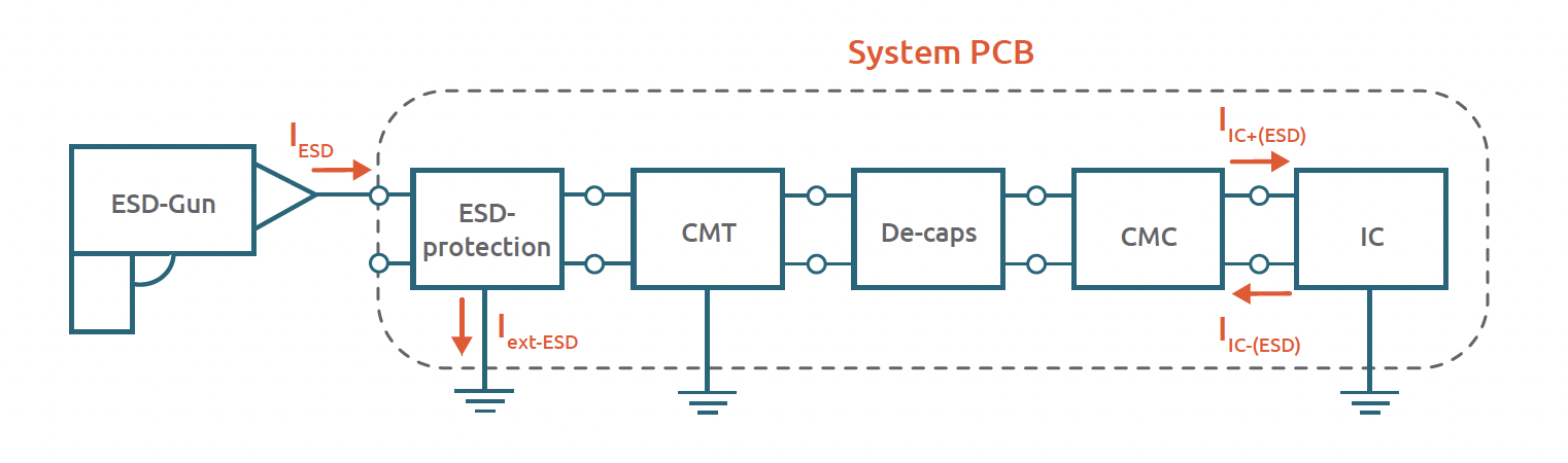
To measure the current that flows into a PHY during an ESD event, a special PCB is recommended by the OPEN Alliance. This test network resembles the Medium Dependent Interface (MDI) in which the PHY is replaced with a resistor network. The network consists of an external ESD device, the common mode termination (CMT) elements, a decoupling network, a common mode choke (CMC), and a 100BASE-T1 PHY (IC).
SEED is developed to perform system-level ESD analysis using transient simulations. To do so, it is essential to have an appropriate model for each part of the target system. Further, to reduce the modelling effort and accelerate the simulation process, a behavioural modelling approach is used. The model, which is tuned to reflect the device’s typical static and dynamic characteristics, is implemented in form of an equivalent circuit consisting of lumped elements, controlled sources and feedback loops, and S-Parameters blocks.
To perform system-level simulations and achieve good agreement with measurements, a model of the ESD generator must be configured and tuned. The parameters of this model are tuned to fit the simulated current waveform on the measured waveform of the ESD generator. Wherever possible, comparisons between simulated and measured time domain current curves in both first and second peak regions of the discharge should be performed, and a good agreement between the simulation and real-world measurements should be observed.
The common-mode termination network and decoupling capacitors are represented in the simulation using lumped elements. The decoupling capacitors separate the IC and the connector pins galvanically, and they protect against slow pulses (e.g., Surge), but not against fast ESD pulses.
The model for the CMC is divided into small-signal and large-signal parts. The small-signal model can be derived from S-parameter measurements of the CMC. A fitted lumped circuit model could also be used in order to speed up the simulation time. Since S-Parameters only enclose the small-signal behaviour, partly including dynamic response and completely ignoring the saturation effect, an extended model should be developed to improve dynamic and include saturation behaviour as well.
For better protection of the IC against high ESD currents, it is important that the external protection triggers before the CMC goes into saturation mode. The high voltage drop across the CMC allows the external protection device to trigger. This means it’s important to ensure that the ESD protection device triggers first. However, it is not sufficient to consider only the static part of the CMC’s IV-curve for prediction of the overall system robustness. The dynamic response of the choke itself plays a crucial role in the validation of the peak currents flowing into the IC during the first peak of the ESD event.
For modelling of the full CMC behavior, the S-Parameter-based CMC model (the small-signal model) is extended with two additional model blocks. The first block is responsible for transition from the static case into the saturation region, whereby the resistance change of the CMC signal through-path is modelled. To realize this, a voltage-controlled changeable resistor (i.e., a voltage-controlled switch) is added in parallel to the main model. For determination of the onset time of the saturation effect, an RC network is used to control the state of the switch in dependence of the input voltage level and rise time.
A feedback loop keeps the switch control circuit in a defined condition throughout the entire ESD event duration. The second block added to the small-signal CMC model improves the representation of its dynamic behaviour, which mainly governs the voltage overshoot generated by the CMC. This is implemented by adding a rise time filter into the signal path of the full CMC model. The overall model is fitted by variation of the parameters related to each model block.
According to the OPEN Alliance specification, the external ESD protection is placed near the system board connector. In this position, it can guarantee a certain robustness level of the overall system, protecting not only the IC but all discrete components located in the signal path.
The static behaviour of the ESD protection device, consisting of leakage, snapback (turn-on), linear and non-linear (thermally unstable) regions, is modelled with the help of voltage-controlled switches and a diode SPICE model. The RC network and feedback loop are responsible for the state of the switches during a second peak of the ESD pulse. The dynamic behaviour of the model is implemented via two RC integration networks combined in such a way as to control the voltage drop over ESD protection as well as its decay time during the first peak of the applied ESD pulse.
The main advantages of the extended dynamic model are correct representation of the thermal behaviour of the ESD protection device and a more accurate description of both the effect of conductivity modulation and inductive overshoot. The conductivity modulation effect is of highest importance for the representation of the voltage overshoot that occurs on the external protection side and will be translated over the CMC to the IC’s I/O pin in the form of peak current.
Once the various parts of the SEED model have been created, the complete system model must be validated against measurements of a reference board with and without external ESD protection using TLP.
A correctly implemented SEED model is suitable not only for qualitative but also quantitative prediction of the overall system-level robustness. Moreover, it can be used for preliminary tests using different system blocks and components. (A more detailed discussion of this topic is available in our whitepaper at https://bit.ly/3jecPpC.)