As e-mobility continues to expand, the automotive industry is presented with many design challenges, like fitting more robust electric motors, controls, and modules into a vehicle while maintaining reliability and signal integrity and reducing weight—where possible—to extend battery life and driving range.
Innovations like the One Pair Ether-Net (OPEN), miniaturization of passive electronic components, and integrated circuit (IC) advancements all contribute to alleviating e-mobility design challenges, but the recent shortages of IC devices have put the spotlight on an occasionally underappreciated element of circuit design—circuit protection. IC shortages will make each module precious and there will be more emphasis to ensure reliable operation in the high transient energy environment that is an automobile.
The urgency for improved circuit protection is compounded not only by the increased quantities of ICs in an electric vehicle, but also by the fact that a common circuit protection implement is a silicon-based device; the transient voltage suppression (TVS) diode. Shortages are expected to impact TVS diodes as well, but the multilayer varistor (MLV) is a viable alternative. TVS technology provides physical, electrical, and cost advantages in circuitry.
In light of possible TVS diode shortages, it is worthwhile exploring the design, performance, and pros/cons of MLVs versus TVS diode technology. The goal is to expand e-mobility solutions preventing overvoltage damage to ICs from electrostatic discharge (ESD), switching transients from inductive loads such as small motors, relays, latches, and servos, and large energy transients like load dump, which is generated after an alternator is disconnected from the battery after starting the engine.
The MLV is constructed in a very similar fashion to multilayer ceramic capacitors (MLCCs), albeit with a different material set. The bulk of the device is a monolithic construction of metal conductive electrode layers and a zinc-oxide-based ceramic. This material is a semiconductor and has non-linear voltage to current characteristics like back-to-back Zener diodes, making it a bidirectional device. At a predefined voltage level, the MLV will begin to shunt current to ground and subsequently clamp voltage to protect sensitive ICs. MLVs can be designed for a wide range of clamping voltages and magnitudes of transient energy. Some additional advancements of MLVs include low ratios of operating to clamping voltage, flexible terminations, 175°C operation, and OPEN Alliance qualified devices that are designed to preserve signal integrity on those lines, in addition to overvoltage protection.
One of the biggest advantages of MLV technology is the extremely high volumetrically efficient active areas that are dissipating transient energy. By comparison, TVS diodes rely on a single P-N junction to clamp voltage. Even if it is a bidirectional diode with two P-N junctions, only one of them will activate during a transient event. The large internal volume of active material becomes increasingly significant for MLVs in highly repetitive transient environments, like an input/output (I/O), human machine interface (HMI), or say a smart combustion chamber that can generate varying magnitudes of sparks based on fuel/air mixture and depending on whether a performance or fuel economy drive is selected.
The multiple layers of an MLV distribute transient energy evenly across all layers, e.g., if there are 10 layers then each layer will dissipate 1/10 of the incoming transient. These layers also provide redundancy if one of the layers begins to degrade making for an extremely reliable device.
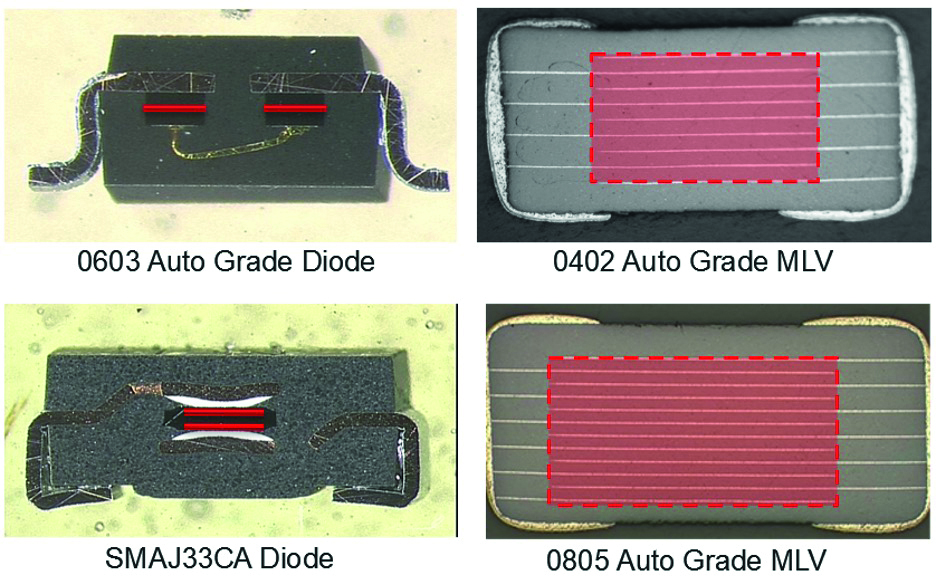
MLVs also require no temperature derating until rated operating temperatures are reached, very much unlike typical TVS diodes that must derate their transient energy capability for anything above room temperature (25°C). This has unique implications for MLV technology in high temperature applications. An EIA 0805 MLV can actually outperform an SMA packaged diode at high temperatures despite being much smaller. You can see this yourself by comparing the datasheets for a SMAJ33CA TVS diode with an energy rating of 0.6J and a 0805 MLV with an energy rating of 0.3J. Although the TVS diode begins at a higher power handling capability, it decays linearly with temperature until the smaller MLV overcomes the diode’s performance at 85°C, again in a much smaller package size.
Reliability across temperature is another parameter that should be considered. Consider a test where a sample of MLVs and TVS diodes were subjected to their 25°C rated peak current transient waveform at 65°C, 85°C, and 125°C. MLVs have no temperature derating up to their maximum operating temperature and had 0 failures when subjected to the same transients across temperature, which was expected. TVS diode failures began at 65°C and were all short circuit failure modes, reinforcing the fact that derating rules for TVS diodes should be strictly followed. Additionally, larger or heat sink-integrated TVS diodes would need to be used to maintain reliability, but size- or cost-constrained designs would benefit from the use of more thermally efficient MLVs.
There are several unique features of MLVs that set them distinctly apart from TVS diodes. MLVs have inherently higher capacitance than TVS diodes, but this quality can be exploited as a dual-purpose EMC capacitor and circuit protection element to consolidate the number of components required to perform the same function. In the case of high-speed signal lines that cannot tolerate capacitive loading, low capacitance designed MLVs would be used. MLVs also have intrinsically low parasitic inductance or equivalent series inductance (ESL), allowing for fast conduction times, thereby suppressing transients as soon as possible.
Some transients are characterized by sub-nanosecond rise times, and impedance contributions by ESL of these devices become significant at these high frequencies. MLVs and many TVS diodes have comparable response times, except for silicon TVS diodes that are wire bonded. These respond slower to suppress fast rise time transients because of higher ESL due to the material, arc length, and the stitch or ball bond of the wire to the silicon die.