The transition to chiplets is a seismic shift that will send shockwaves throughout the industry.
Highly integrated monolithic semiconductor devices have provided a stable foundation for rapid innovation in the electronics industry for many decades now. However, that foundation is starting to show signs of cracking as a new wave of chiplet- based devices begins to take hold. Understanding the significance and implications of chiplets will be critical for successful design development in the future, particularly for the rapidly-growing edge IoT and AI/ML markets.
How chiplets came to be
The use of chiplets can be traced back to the growing complexity of electronic systems. To support this tendency, monolithic semiconductors have correspondingly become more complex, with the largest devices being built today incorporating more than 100 billion transistors. However, building ever larger and more complicated devices creates a host of issues including long design and verification times, high development costs, high device costs, and thermal management problems. A powerful solution to that problem is to modularize the design, development, and production of devices by means of chiplets.
Benefits of chiplets
Chiplets, which may also be known as tiles, offer many benefits, including the following:
Modularity and scalability:
Chiplets enable a modular approach to chip design. Instead of integrating all functions into a single monolithic device, IC designers and their customers can use separate chiplets for specific functions. This modularity enhances scalability, simplifying the process of upgrading or customizing electronic systems.
Improved yield and cost efficiency: In traditional monolithic IC manufacturing, a defect in one part of the chip renders the entire device unusable. With chiplets, if a single slice of silicon is defective, only that chiplet is unusable. The result is higher yields and lower total device costs.
Shorter time-to-market:
The modular nature of chiplets enables parallel and independent development of individual components, leading to shorter design and development cycles and a reduced time-to-market. This is a critical advantage in a world where AI design, models, and algorithms are rapidly evolving.
Reusability of proven standards-based chiplets:
This reduces the risks as well as the development costs and time of new product variants.
Enabling technologies
One of the most important enablers of chiplet adoption is efficient interconnect technologies. Advanced packaging techniques (e.g., 2.5D and 3D stacking) play a crucial role in connecting chiplets seamlessly. These technologies enhance signal integrity, reduce power consumption, and enable the creation of more compact electronic systems. However, complementing these physical packaging approaches with an electrical chiplet-to- chiplet interface standard would further catalyze the adoption of chiplet technology. Fortunately, such a standard has recently emerged through a broad industry effort.
Enter UCIe
Universal Chiplet Interconnect Express (UCIe) has emerged as a pivotal development in the realm of chiplets, serving as a standardized interface that facilitates seamless communication and integration among diverse chiplets within a system. By providing a common language for chiplets, UCIe ensures interoperability, allowing designers to effortlessly connect different components, such as CPUs, memory, AI/ML blocks, A/Ds, DSPs, high-performance I/O modules, and other specialized functional blocks.
The UCIe specification covers the die-to-die physical layer, communication protocols, and software stack, leveraging the PCI Express (PCIe) and Compute Express Link (CXL) industry standards. Two versions of the specification (1.0 and 1.1) have already been published and are available on the UCIe public website.
Having an open standard approach not only simplifies the design process but also promotes a more modular and scalable system architecture. As industry giants including AMD, Arm, Google Cloud, Intel, Meta, Microsoft, Qualcomm, Samsung, and TSMC rally behind UCIe, its position as the preferred interconnect standard has solidified, setting the stage for collaborative ecosystems, and fostering innovation in chiplet technology.
Heterogeneous integration
Chiplet-based development approaches allow disparate technologies to be integrated into a single device, thereby engendering several benefits. For instance, a chiplet-based system can easily combine analog and digital components, components built on different process geometries or process types, or those that have different physical dimensions or pad pitches. This heterogeneous integration allows a “mix-and- match” flexibility that is simply not possible with monolithic devices, thus creating an environment conducive to rapid innovation. Certain technologies, such as analog subsystems and non-volatile memory, do not easily scale to advanced nodes, so keeping cost-optimized, proven chiplets in older process nodes results in lower risk, shorter time-to- market, and lower unit costs.
AI possibilities
AI and ML functionality is increasingly becoming integral to the development of leading- edge electronic systems. Chiplets offer a platform for integrating specialized AI processors, enabling devices to perform complex tasks with higher efficiency and performance. They also provide a mechanism for rapidly tailoring devices to particular use cases among a diverse range of potential AI applications, such as edge IoT predictive maintenance or cloud-based image recognition. Ultimately, developers will likely be able to choose from among processor, memory, and peripheral options to create devices that meetspecific cost, performance, and power requirements.
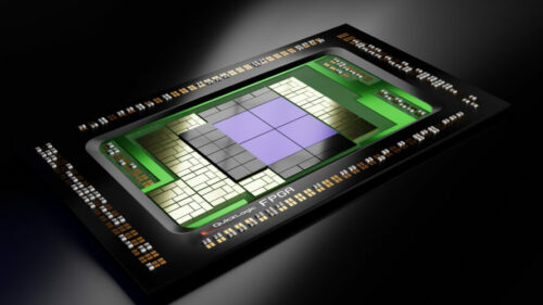
FPGA technology
Another key technology enhancing the use of chiplets is programmable logic, particularly FPGA fabric
that has been designed for easy chiplet integration. One example of such a device comes from a collaboration between YorChip and QuickLogic. This strategic partnership aims to create a lineup of FPGA-based chiplets optimized for low power consumption and low cost.
For example, one chiplet comes with four x16 UCIe ports and approximately 40K LUTs of FPGA logic, combining terabit/s I/O interconnect bandwidth with high-performance, low latency, and low power FPGA fabric. Target markets include edge IoT, AI/ML, automotive, military, aerospace, industrial, and medical applications.
Benefits of chiplets
FPGA chiplets offer several benefits over traditional monolithic devices including:
- Smaller size.
- Lower power consumption.
- Lower unit costs.
- Increased flexibility.
- Shorter time-to-market.
- Reduced development costs.
Using a chiplet-based approach enables developers to create variable sized two- dimensional arrays of FPGA chiplets to quickly scale gate counts (up or down) and to add other functions, including dedicated processors, memory and peripheral devices. Designs targeting each chiplet could be developed independently and in parallel to reduce time-to-market.
Market projections
According to MarketsandMarkets, a leading market research firm, the adoption of chiplets is expected to grow from a Total Addressable Market (TAM) of $6.5B in 2023 to $148B in 2028—a compound annual growth rate of 86.7%. The anticipated growth spans a range of markets, with UCIe-enabled chiplets expected to be a key factor.
The future of chiplets
Currently, the largest impediment to the broad adoption of chiplets is availability of the chiplets themselves. Many companies, including several of those listed as driving the development of the UCIe standard, are already testing and evaluating the technology with an eye toward near-term productization. Other companies are springing up to act as third-party chiplet enablers working in tandem with chiplet suppliers.
FPGA chiplets will act as a flexible glue to help mix and match disparate chiplets for system developers while adding design flexibility and advanced security features. Given their inherent flexibility to address a broad set
of applications, it seems likely that chiplet adoption will grow dramatically over the next few years.