Performance and reliability come as standard with Innoscience.
Gallium nitride (GaN) is now widely used in a variety of applications, including chargers and adapters for mobile phones where it delivers efficiency and power density benefits, as well as in other sectors such as automotive, data centers, LED drivers, renewable energy, consumer, audio and phone handsets, for example. Engineers have realised that GaN’s superior switching performance is suitable for countless applications, and they are growing increasingly confident in the ability of suppliers like Innoscience to deliver proven technology combined with rugged and qualified processes—not to mention massive capacity.
Innoscience is the world’s largest manufacturing company fully focused on 8-inch GaN-on-Si technology. From the very beginning, Innoscience management understood that, for GaN technology to become ubiquitous in many markets, performance and reliability—whilst vital considerations—were only a starting point.
Before GaN could become widely adopted, customers would have three additional key demands. First, that GaN technology devices must be affordable as the industry isn’t willing to pay a big premium. Second, a large manufacturing capacity is necessary in order to deliver large volumes and absorb demand fluctuations. And third, customers require security of supply, allowing them to develop their products and systems using new GaN devices safe in the knowledge there won’t be production discontinuations and shortages.
Innoscience executives understood that only by focusing on 8-inch GaN-on-Si technology, by dramatically scaling-up GaN-on-Si device manufacturing, and by controlling its own production fabs would it be possible to meet the requirements of the electronic industry (namely: price, volume, and security of supply).
Innovative technology
Let’s look at the technology Innoscience has developed together with its trusted international partners. Power semiconductor engineers demand devices that show a normally-off operation; i.e., no current conduction when the transistor’s gate is set at 0V. Since the natural form of GaN HEMTs (High Electron Mobility Transistors) is normally-on (so-called depletion mode), special drivers must be placed in cascode package solutions to realize normally-off operation.
However, Innoscience’s GaN HEMTs are intrinsically normally-off (enhancement mode) devices. Normally-off operation is realized by growing a p-GaN layer on top of the AlGaN barrier, forming a Schottky contact with the p-GaN layer. This increases the potential in the channel at the equilibrium, resulting in normally-off/e-mode operation.
Low specific RDS(on)
A key parameter for defining device performance is the specific RDS(on), the on-resistance per unit area. The lower the specific RDS(on), the smaller a device can be made, enabling more devices per wafer and lower device cost.
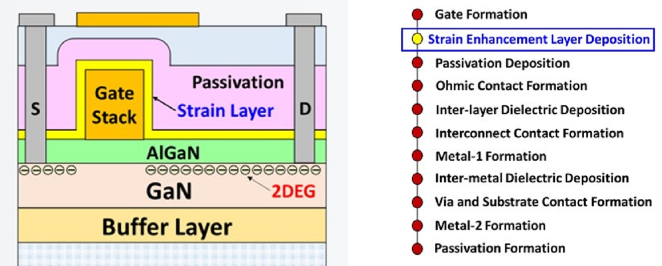
Innoscience developed a proprietary strain enhancement layer technology, which consists of the deposition of a specific layer after the gate stack definition. The stress modulation created by the strain enhancement layer induces additional piezoelectric polarizations, which cause the 2DEG density to increase reducing the sheet resistance by 66%. Since the strain enhancement layer is deposited after the gate formation, it affects the resistance only in the access region and it does not impact other device parameters such as threshold and leakage, etc.
Therefore, Innoscience’s GaN-on-Si e-mode HEMTs show very low specific on-resistance. Because Innoscience has optimized both epitaxy as well as device process technology, the (dynamic) RDS(on) does not increase over the full temperature and voltage range, suiting it for power switching applications.
Today, Innoscience can produce more than 10,000 8-inch GaN-on-Si wafers every month; this will increase to 70,000 wafers per month by 2025. The first Innoscience fab is already qualified to ISO9001 and the IATF 16949:2016 certification for automotive use. These GaN HEMTs are also qualified to the JEDEC standard as Innoscience performs more advanced reliability tests to verity its devices.
Conclusion
Uniquely for a GaN company, Innoscience offers devices that cover the low voltage (30-150V) and high voltage (650V) range. Innoscience’s GaN HEMTs (InnoGaN) are available from 30-150V in chip scale packages (CSPs) measuring 2x2mm to 2.2×3.2mm with RDS(on) as low as 5.5mΩ (typical). Furthermore, 650V parts in DFN and wafer scale feature RDS(on) levels as low as 106mΩ (typical). Innoscience GaN HEMTs are being used in USB-PD chargers up to 120W and in LLC converters. They are also to be found inside data center power supply racks.
By combining world-class technology, state-of-the-art processing technology, and the world’s largest 8-inch GaN-on-Si capacity, Innoscience is answering both engineering and commercial challenges, enabling designers working in all market sectors to benefit from proven performance benefits with no cost penalty.