Edge AI SoCs get all the attention, but don’t forget the development tools.
It seems everything is moving to the Edge. Product developers tout the ability to perform very sophisticated artificial intelligence (AI)-enabled processing at extremely efficient power consumption levels—far from the processing resources of centralized computing architectures. Armed with these solutions, designers are free to create a new wave of low-power AI-enriched solutions targeted at the edge of a network. Now, products designed for both embedded industrial and consumer applications can make decisions locally without relying on a cloud connection.
With this decentralized processing approach, end users benefit from faster response times, enhanced privacy and security, and better use of available wireless bandwidth. It also allows these devices to run off AAA or even coin-cell batteries for extended periods, liberating them from the constraints of line power.
However, this wave of innovation around edge AI has put designers in the position of needing to quickly develop products for a rapidly changing technology landscape. Their designs rely on both the sophistication of AI and its ability to be deployed quickly at the network edge, where it can make intelligent decisions based on data from multiple sensor inputs using accurate and specifically-trained AI models.
Giving designers a helping hand… and a good night’s sleep
Developing AI-infused products can quickly become challenging. A well-thought-out evaluation and design development platform can greatly simplify a development cycle by removing many, if not most, of the time-consuming, headache-inducing steps.
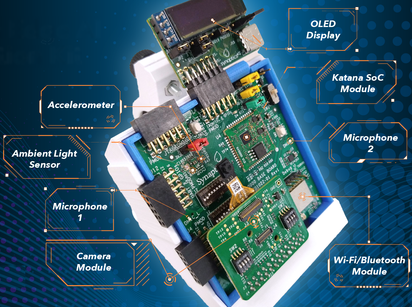
This is especially true for system-on-chip (SoC)-based designs. As their name implies, SoCs combine a range of essential yet previously separate functions into a single, efficient chip. In the case of the Synaptics Katana Edge AI SoC, for example, those functions include advanced processing, connectivity, audio and video input and output, power sources and, of course, intelligence, based on proprietary neural network technology.
This type of complexity clearly underscores the need for comprehensive development tools. Such aids factor heavily into streamlining the design process, saving time and resources, and getting products to market as quickly as possible.
EVKs simplify Edge AI development
Edge AI products built around SoCs represent some of the most sophisticated designs in use. Because of the diverse applications those devices target, their development platforms have to be as complete as possible. The evaluation kit (EVK) that was recently introduced for Katana, as an example, contains not just the base board with the SoC, a multitude of sensors and a Wi-Fi/Bluetooth wireless connectivity module, but also individual accessory boards for a range of duties, such as a camera, as well as peripheral extensions, and a power source. Cables, batteries, and enclosures round out the EVK.
The AI algorithms in EVKs like this can enable sophisticated features in SoCs, such as person “fall detect” for home healthcare and assisted living monitoring, as well as counting people for applications in smart buildings, theaters, and stadium crowd control.
The helping hand to transform SoCs from chip to solutions
SoCs at the heart of the edge AI revolution, along with the development tools supporting them, are looking at a bright future. Anand Joshi, managing director of AI analysis firm JD Data observes that SoCs’ wide variation in power, size, performance, and degree of functional integration in embedded and IoT systems pose particular challenges to designers. The costly time delays inherent in fragmentation—disparate hardware and software pieced together into a makeshift development platform—can be mitigated, he says, with proven EVKs.