The idea of smart cities really began when communication of information between individuals became commonplace. It wasn’t until the IoT took off that the idea of smart cities gained traction along with applications justifying infrastructure change.
There are many practical applications that can improve quality of life and municipal operations, such as optimizing traffic patterns and improving safety in the form of natural disaster response and criminal investigations. Other improvements might include applications to increase energy efficiency by way of lighting, distributing grid power, and even energy generation.
Timing must also be considered. The GPS location of an asset, transactions, utility meter readings, self-driving cars, etc. all require a temporal reference for the information to be meaningful during analysis. A smart city will require sundry wireless nodes (consider V2X communications), sometimes operating in harsh environments or presented in small packages, and critical to these modules will be oscillators.
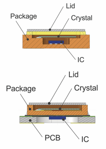
In the case of conventional structure oscillators that are being used by many suppliers today, the quartz crystal and associated integrated circuit (IC) are both housed in a ceramic package sealed with a metal lid. These devices typically range from EIA Metric 7050 (7mm x 5mm) to 2016 (2mm x 1.6mm) case sizes. This means that for every case size in-between, there is a unique ceramic package, crystal, and IC interface that must be accounted for in the design to resonate reliably at a given frequency. These designs are all well and good, but there are benefits to removing the IC from the proximity of the crystal, so long as there is packaging and crystal processing proficiency to maintain frequency performance.
A new and novel packaging method for the quartz and IC of an oscillator—known as a “platform structure oscillator”—will enable longer life, provide higher reliability, and reduce costs, possibly lowering processing costs as well.
Using this approach, only the crystal is housed within a 2016 case size ceramic package, which is also known as the “head unit.” This allows for a high-temperature annealing process that would not be possible if the IC was present. The main purpose of the annealing process is to enhance the aging characteristic of the crystal, but this process also prevents packages from having contamination that may lead to failures.
The ceramic package is then soldered to a PCB (the “platform”) that contains the IC. The 2016 case size of the package doesn’t change, which makes it cost effective from a manufacturing viewpoint, while the PCB can be any size from 2016 to 7050 as a drop-in replacement for conventional oscillators or to provide an option for future size reductions while using the same head unit. The PCB platform also absorbs any coefficient of thermal expansion (CTE) mismatch from the ceramic package to the circuit board.
Advancements in crystal formation, processing, and cutting allow for a wide range of designs in smaller sizes. Packaging advancements contribute to a solid interface from the package to the IC that reduces leakage currents, which will be a big parameter for all components when considering the sheer number of smart city modules. Component innovations like these will enable the creation of modules with longer, more reliable lifetimes that can endure harsh environments as efficiently as possible.