Earlier this week, an electrical engineering student (the son of one of my friends in whose home a small group of us meet once a week to spend an evening watching Doctor Who) asked me a question.
It seems his class has been learning about some of the tools we use to design integrated circuits (ICs) and printed circuit boards (PCBs). His question was, “How will engineers design electronic products in the future?”
Unfortunately, although I love to expound, explicate, and elucidate (much like my dear old mother, the real trick is to get us to stop talking), I couldn’t answer this in any depth at the time because Doctor Who was calling, so I decided to gather my thoughts in this column.
How Things Were
Let’s start by considering how things used to be. My first position after graduating from university in 1980 was as a member of a team designing central processing units (CPUs) for mainframe computers. This was also my first experience of designing application-specific integrated circuits (ASICs). These were Toshiba devices implemented at the 5-micron (µm) process node, where “5µm” refers to the size of the structures used to create the transistors on the silicon substrate (microns are 1,000 larger than the nanometer (nm)-scale transistors we work with today).
Our design tools in those days of yore were pencils and paper. We created our schematic (circuit) diagrams as netlists of logic gates and registers. When it came to timing verification, we identified the critical paths by eye and then summed the gate and wire delays by hand (no one I knew could afford even a 4-function handheld electronic calculator). In the case of functional verification, you gathered the rest of the team, who sat around the table perusing and pondering your schematics while asking probing questions about your design along the lines of “What does this bit do?” and “Why did you do things this way rather than that way?”
Around this time, I had friends who were creating printed circuit boards (PCBs) using the “Dot and Tape” method. The idea here was to “draw” the tracks by attaching sticky tape to a transparent mylar sheet. The “dots” were annular rings with various inner and outer diameters made from the same material as the tape. Collections of these pads matching integrated circuit (IC) pin patterns were also available. The layout designers worked at 2:1 or 4:1 scale. When they were finished, a photograph was taken of the layout, and this was subsequently projected into the board at 1:1 scale as part of the process of etching the photoresist and then etching the copper.
Over time, computer-aided engineering (CAE) tools were developed to help design engineers perform tasks like schematic capture and circuit simulation (both analog and digital). Similarly, computer-aided design (CAD) tools were developed to help the layout designers to place the components and route the tracks on the PCBs.
One important aspect of all this is that very few people were developing ASICs at that time. The majority of engineers in the 1980s were working on PCBs containing large numbers of simple off-the-shelf ICs and discrete (individually packaged components).
How Things Are
Engineers designing electronic products today are equipped with an array of sophisticated design and verification tools. At the PCB level, for example, design engineers have access to incredibly sophisticated schematic capture technology integrated with tools like search engines that aggregate parts from distributers and inform the designers as to component availability in real time. Meanwhile, the tools used by layout designers can take a good first pass at automatically laying out the board, including tasks like the impedance-matching of differential signals. The designers can then “tweak” the layout, pushing and shoving tracks and vias while the system automatically re-routes surrounding tracks and vias in real-time. All of these tools are augmented by sophisticated timing analysis and simulation engines (analog, digital, and mixed-signal) coupled with powerful analysis and verification tools, like signal integrity (SI) and power integrity (PI).
For those designing ASICs, the latest and greatest devices are known as system-on-chip (SoC) components. These integrate most or all of the functions of a computer or other electronic system, including one or more processor cores, memory blocks, and accelerator, communication, and peripheral functions.
These functional elements are referred to as intellectual property (IP) blocks. In the early 1990s, an entire SoC might boast a few tens of IP blocks and contain “only” 20,000 to 50,000 logic gates. Today, an SoC can contain hundreds of IP blocks, where an individual IP block—say a USB communications function—can contain hundreds of thousands of logic gates.
Some incredible tools are available to design and verify devices of this complexity, including high-level synthesis (HLS) in which designers essentially describe what they want at a high level of abstraction and the tool translates this into the netlist of gates and registers that will achieve the specified requirements (size, performance, power consumption…).
Another consideration is how all these IP blocks should be connected together. SoCs in the early 1990s predominantly used similar bus structures to those employed by PCB designers. In this case, all of the IP blocks were connected to a common bus. The terms “initiator” and “target” are used to refer to IP blocks that initiate or respond to transactions, respectively. Typically, there would be only one (or very few) initiators, like a single CPU, talking to a bunch of targets.
By the early 2000s, SoCs typically contained a bunch of initiators and a bigger bunch of targets (please forgive my use of tongue-twisting technical terms like “bunch”). Simple bus structures weren’t capably of handling devices of this complexity because all the IPs would end up waiting for the other IPs to do their “stuff.” To address this, designers started to use crossbar switch architectures, in which any initiator could talk to any target and multiple transactions could be “in flight” at any particular time.
In the case of today’s designs, even crossbar switches have run out of steam. For example, I was recently talking to the folks at a company called SiMa who have designed a machine learning (ML) device they call a MLSoC. This little scamp contains close to 5 billion transistors! In order for this to work, they are using something called a network-on-chip (NoC), whereby initiators and targets talk using “packets” of information, similar in concept to the way in which the internet works.
The MLSoC contains hundreds of IP blocks, some developed internally along with many from third-party vendors. One interesting point here is that the design team at SiMa didn’t want to create a NoC themselves; instead, they wanted to focus their efforts on developing their own “secret sauce” IP blocks that differentiate their product from the competition. Thus, they turned to the guys and gals at a company called Arteris, who have a powerful and proven solution in the form of their FlexNOC Interconnect IP.
How Things Will Be
Many of the people who see the title of this column will think about the people and tools used to design the hardware portions of an electronic product. However, todays electronic systems—especially embedded systems—also contain copious amounts of software.
GitHub is an internet hosting platform for software development and version control. It is commonly used to host open-source software development projects. As of June 2022, GitHub reported having over 83 million developers and more than 200 million repositories, including at least 28 million public repositories.
The reason I mention this here is that GitHub has developed something called Copilot. This uses artificial intelligence (AI) that has been trained on billions of lines of existing code to help software developers create their programs. Using their favourite editor, after selecting the programming language they wish to work in, the developers can type a comment (e.g., “This function counts from 0 to 87 and then stops”) and Copilot will immediately start suggesting code. Even without comments, if the programmer starts typing code, CoPilot will start offering suggestions. I have one C/C++ programmer friend who says Copilot has boosted his productivity by an order of magnitude. Another friend who creates field-programmable gate array (FPGA)-based designs says that Copilot also works with hardware description languages (HDLs) like Verilog and VHDL, which are used by FPGA, ASIC, and SoC designers to capture their design intent.
Now, we are starting to see the first toes being dipped into the waters of AI-enabled hardware design. In one example I’ve seen, when a design engineer commences work on a portion of a PCB design, the system’s AI (which has been trained on hundreds of thousands of existing designs) can immediately start making suggestions. In fact, it seems inevitable that AI will start to pervade all aspects of electronic hardware and software design, analysis, and verification in the not-so-distant future.
It’s not so long ago that whenever anyone wanted to design anything, they had to design everything from scratch. As an example, consider the Austrian-born American inventor and businessman Heinz Joseph Gerber who pioneered computer-automated manufacturing systems for an array of industries. In the 1960s, Gerber started work on digital drafting and plotting tables, which ended up being used for all sorts of things, including designing PCBs. He needed some standard format to store his digital plotting data, but there was no such standard, so he created his own, which we now call Gerber format and use to this day.
Designing everything from the ground up is a hard way to do things. These days, it’s possible to create new hardware and software products by gathering existing well-defined “chunks” together. There are also amazing tools available that allow engineers to develop awesome products by using a graphical user interface (GUI) to drag-and-drop design elements and connect them together. For example, a company called DSP Concepts has a product called Audio Weaver.
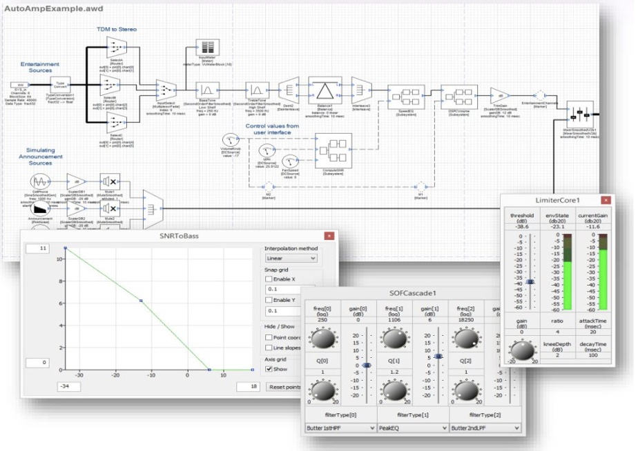
You can read more about this in my column, You Too Can Rule the AoT with Audio Weaver. By some strange quirk of fate, I was recently introduced to a company that is working on a similar scheme for creating AL/ML based systems. Currently, relatively few engineers have implemented any form of AI/ML system because doing can be incredibly complicated.
More recently, tools have started to appear that makes this sort of thing much easier. For example, the folks at Cartesiam (now part of STMicro) have developed a product called NanoEdge AI Studio that helps developers to create AI/ML apps that run on low-power microcontrollers on the edge (i.e., the boundary where the internet meets the real world). In fact, I created such an app myself (and if I can do it, anyone can do it). You can read about this in my column I Just Created my First AI/ML App!
Funnily enough, just a couple of days ago as I pen these words, I was talking to a company that is poised to launch a new AI/ML chip supported by a drag-and-drop GUI that will allow designers to create AI/ML products by simply connecting blocks together, where these blocks have names like Grab Image > Perform Face Detection > Crop Image to Face > Perform Face Identification… and so forth.
Another thing that will change design is the way we interface with our tools using augmented reality (AR) systems. We’ve all seen science fiction films like Minority Report featuring Tom Cruise using AR interfaces. Well, real-world versions of these AR interfaces are coming our way, and they will be here sooner than you think. We already have most of the parts in place. One of the main things holding us back has been affordable (consumer-grade) AR glasses, but a number of companies are making tremendous strides in this area, such as TriLite Technologies whose glasses-mounted AR laser display is less than one cubic centimetre in volume (see my column How Long Until We See Whales in Classrooms?).
But Wait, There’s More
Sadly, I fear we have only scratched the surface of this topic, because I have so much more I want to talk about but so little time to do so.
Furthermore, in addition to cogitating on how engineers will design electronic products in the future, we might also want to ruminate on what sort of electronic products they will be designing.
Happily, these are all topics that we will be covering in future issues of DENA, which means it would be a really good idea for you to register for your free subscription today, and also share this news with your friends and colleagues. As always, I welcome your insightful comments, perspicacious questions, and sagacious suggestions (you can contact me at [email protected]).