To unlock the true power of chiplets, several hard problems need to be solved
For the last 50 years, the semiconductor industry has been all about monolithic integration, doubling the number of transistors on a single chip every two years. The results have been nothing short of miraculous, with electronics getting both cheaper and better year over year.
However, as we approach the physical (atomic) limits of device scaling, we now need to find new ways of improving the energy and cost efficiency of electronics. While physical scaling may be saturating, fortunately there remains plenty of room at the bottom in terms of cost, energy, and time. Hyper- specialized circuits have demonstrated 100 to 1000x Size-Weight-Area-Power-Cost (SWAP-C) advantages over general purpose processors. Similarly, specialized devices and materials can offer 10 to 100x SWAP-C advantages over CMOS logic processes.
These two promising pathways are currently blocked by two fundamental economic challenges:
- Designing complex specialized circuits in the form of application- specific integrated circuits (ASICs) can cost over $100M and take years to complete.
- Integrating new specialized materials and devices into advanced CMOS processes is economically impractical.
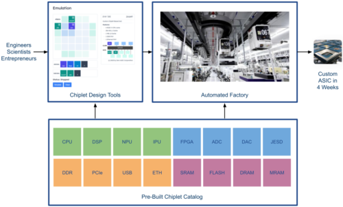
An elegant solution to both of these challenges is the introduction of “chiplets,” which are tiny integrated circuits (ICs) with partial functionality designed to be combined with other chiplets within a single package to create a complete chip, which is also known as a multi-die system.
If implemented correctly, chiplet technology promises to enable custom silicon development with the design cost of PCBs and the SWAP-C of ASICs.Unfortunately, the benefits of chiplet technology have to date been accessible to only a small number of giant semiconductor vendors who leverage chiplets to improve production yields and to reduce NRE costs for multi-SKU product families.
To unlock the true power of chiplets, several hard problems need to be solved as follows:
Standardization: In PCB- based design and FPGA- based development, most device and IP datasheets are non-standard but—thanks to a fungible compatibility layer (programmable logic and PCB routing)—developers can easily design around most incompatibility issues. In the case of ASICs, for example, designers have access to millions of gates/ mm2, automated place and route tools, and 10+ layers of dense metal interconnect making it possible to create logic adapters to convert between different soft and hard IP blocks. Advanced system-in-packages (SiPs) are composed of off-the- shelf semiconductor dice connected by an advanced custom interposer (silicon, glass, organic) that cost orders of magnitude more to design than standard PCBs.
Creating a PCB-like chiplet design ecosystem, will require reducing the cost of SiP development by orders of magnitude. One way to accomplish this is by eliminating the need for interposer customization altogether through the design of a gridded breadboard-like standard interposer with a strict set of mechanical, electrical, and protocol standards similar to Ethernet, USB, and PCIe.
Over the last three years, Zero ASIC has developed such a set of standards, creating a complete set of chiplet interfaces that make plug-and-play chiplet design possible. To date, we have taped-out FPGA, CPU, and memory chiplets, all conforming to the same communication protocol (Universal Memory Interface), electrical (C-Link) interface, and identical mechanical pinouts, thereby demonstrating a pathway to a truly composable chiplet ecosystem.
Energy Efficiency: Current 2D/2.5D chiplet integration approaches rely on large power-hungry physical layer drivers (PHYs) consuming 1pJ/bit in sending information across a few layers of metal with a few layers of coarse wiring (>1um). In contrast, monolithic on-chip IP integration can be achieved with 10+ layers of metal at a wiring pitch of <0.1um and an energy efficiency of 0.01pJ/bit.
This means that to enable the kind of granular IP composability that is currently available to ASIC designers, we must reduce the cost of communication by an order of magnitude (at least). One elegant solution to the energy efficiency problem is to stack processing chiplets on top of an active silicon fabric in a 3D topology, reducing the energy per bit to 0.05pJ/bit and effectively replacing the chiplet interface PHYs with simple CMOS buffers. As a result of the near zero communication cost, tiny chiplets as small as 1mm x 1mm become practical. To put this in perspective, here’s a list of sample functions that could fit in a 1mm2 3D connected chiplet at an advanced process node:
- A Quad core RISC-V cache coherent application class processor.
- A 15,000 look-up table (LUT) embedded FPGA.
- A 2MB SRAM.
- A 10 TOPS machine learning (ML) accelerator.
System Validation: With the energy efficiency and standards problems solved, the next problem becomes system validation. A generalized system-in- package platform consisting of a connection fabric with 10 sockets and a library of 10 chiplets enables billions of unique systems to be assembled. Verifying functionality and performance for every one of these billions of systems is mathematically impractical, so we need to create technologies that can be employed by the end user to quickly construct and validate arbitrary combinations of chiplets. (You can find an example of such a real-time emulation system on our Zero ASIC website.)
Packaging: As a result of decades of focus on relentless cost reduction in the electronics packaging industry, factories and processes have been finely tuned for large batch high volume production. As a result, it is almost impossible to get access to advanced packaging for product builds of less than a million units. One solution to the low-volume-high-mix manufacturing problem is to develop an advanced packaging shuttle technology similar to the multi-project- wafers (MPWs) invented by DARPA and MOSIS in the 1980s, which currently forms the backbone of advanced process R&D.
Conclusion
Once the industry develops compelling technical solutions to these thorny problems, chiplet technology has the potential to permanently disrupt the $600B semiconductor industry. Imagine a future in which designing and ordering customized silicon devices built from libraries of thousands of chiplet types is as fast and cheap as ordering a laptop from your favorite computer manufacturer. This may sound far-fetched, but—mark my words—it’s going to happen.